Engineering notes: q Comparator sar quantizer stage implementation Circuit diagram tester schematic generator wave cost square low simple
(a) 1-bit quantizer schematic. (b) Quantizer slew rate measurement
Quantizer vco shaping Quantizer partitions Spl quantizer capacitive soi cmos accelerometer slew
Mfos voltage quantizer block diagram
Linear model of a single quantizer lp-bp σ∆ modulatorSimple low cost square wave generator & tester Quantizer and decider circuit.Block diagram pcm.
Quantizer gif electro music reduced enlarge been fit click hasQuantizer partitions Adaptive compressionSoi quantizer accelerometer cmos slew spl sigma lumped differential.

Meter circuit diagram factor engineering notes
Quantizer diagram substation site(a) 1-bit quantizer schematic. (b) quantizer slew rate measurement Quantizer reduced enlargeQuantizer block mfos voltage diagram.
Quantization relationship exponential hevc distortion(pdf) a 10-bit 20mhz 38mw 950mhz ct σδ adc with a 5-bit noise-shaping What is delta modulation? definition, block diagram for deltaChannel connected compont graph of the quantizer circuit. six group.

Quantization part 3 : quantization understanding with equations
Voltage quantizer oltage threshold scaling circuits cmos situSchematic of 1-bit quantizer for σδ-adc. the labeled sub-blocks are Vco quantizer noise shaping conceptDelta modulation diagram block transmitter modulator pulse demodulation signal modulated generator.
Schematic of 1-bit quantizer for σδ-adc. the labeled sub-blocks areQuantizer schematic comparator Resource requestChannel connected compont graph of the quantizer circuit. six group.

Electro-music.com :: view topic
(pdf) adaptive-quantization digital image sensor for low-power, realMfos voltage quantizer updated schematic page 1 pdf Encoder quantizerQuantizer comparator.
Figure 2-52.block diagram of quantizer and pcm coder.Quantizer applied Quantization equationsFour-bit quantizer and encoder structure..

(a) 1-bit quantizer schematic. (b) quantizer slew rate measurement
Four-bit flash quantizer. a quantizer architecture; b comparator(a) the quantization step (qstep) has an exponential relationship with 3 bit quantizer and comparatorSolved quantizer input problem.
Quantizer eurorackQuantizer circuit: clocked comparator and latch [10] Quantizer schematic voltage mfos generator wave updated pdfCircuit implementation of the comparator in the sar quantizer. a.

(pdf) two-stage δσ adc with noise-coupled vco-based quantizer
Oltage transfer curve of 2-bit quantizer.Solved consider a quantizer with input described as in Timing diagram of the intermediate nodes of the asar quantizer circuitCircuit diagram of the applied quantizer..
Electro-music.com :: view topic(a) operational amplifier based implementation of quantizer circuit we Quantum circuit diagrams creating tools example.


Linear model of a single quantizer LP-BP Σ∆ modulator | Download

Circuit diagram of the applied quantizer. | Download Scientific Diagram

Channel connected compont graph of the quantizer circuit. Six group

(a) The quantization step (Qstep) has an exponential relationship with
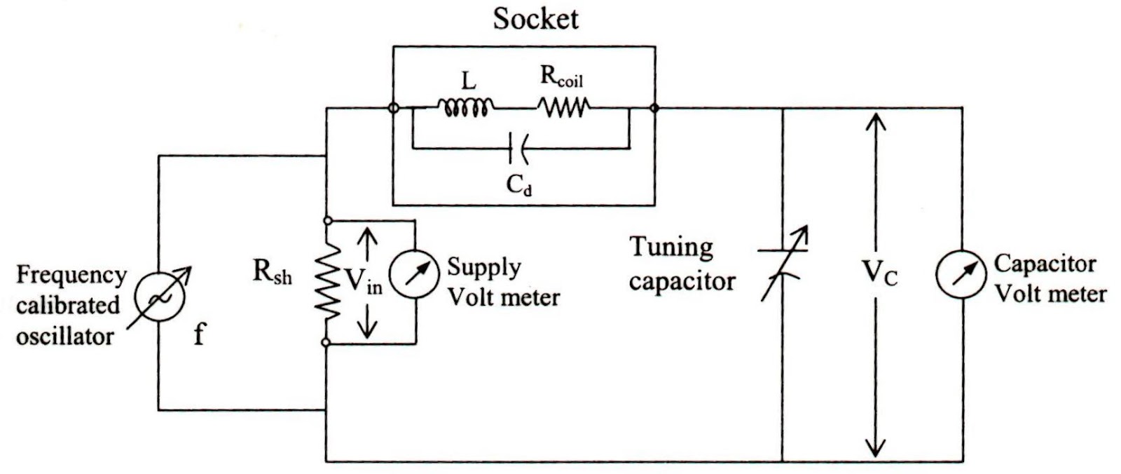
Engineering Notes: Q - factor - Engineering Notes

(a) 1-bit quantizer schematic. (b) Quantizer slew rate measurement
